Induction Heater Inverter Schematic
PLL OVERVIEW
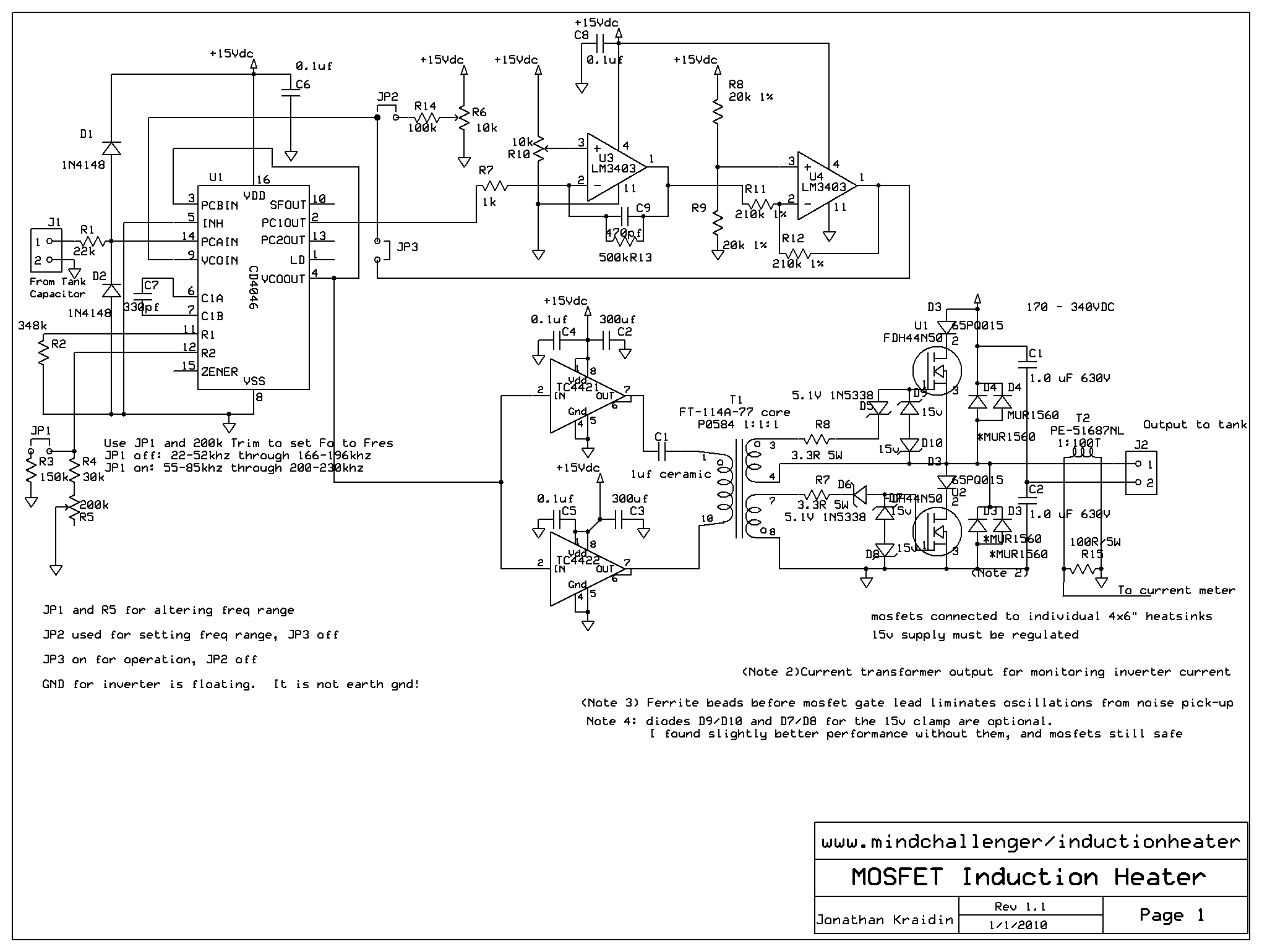
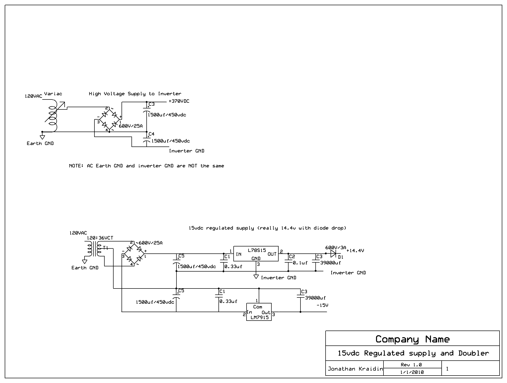
The PLL receives two inputs through pins 14 and 9. Pin 14 is the clamped capacitor tank voltage. It is inverter (shifted 180 degrees) in order for the feedback to work properly. The high voltages are kept down with R1. All inverter grounds are isolated from earth ground. C7 and resistors on pins 11 and 12 set the capture range. Jumper JP1 converts pin 12's resistor from 100k to 60k. R5 affords you the ability to vary the capture range even more for tuning the center frequency to the tank resonant frequency. We will discuss this at the end.
PCAout goes through the active integrator filter, which is made up of a quad op-amp. The integrator output then goes through a filter with a gain of -1 to restore the polarity of the signal. During use, jumper JP2 is open and JP3 is closed to allow the feedback to get to pin 9. The drive frequency leaves pin 4 and drives a non-inverting and inverting gate drive. These chips drive the primary of a 1:1:1 gate drive transformer, T1. C1 removes DC bias. Diodes D5 and D6 offer some delay so both mosfets are not on at the same time. These series diodes have nothing to do with reverse currents, like the one's you are used to seeing across the DS juntion. Again, they are for timing. Your tracings should be short to the gate drive on the mosfet. I have connectors on my board going to wires which run to the chips on large heat sinks. The wire acts like an antenna and you can get noise which will induce wild oscillations in your mosfets, destroying them. I put a ferrite bead that attenutes frequencies above 300khz right before the lead to the gate drive. This works perfectly. Below are the tracings going to the gates and then showing the tracing from one of the gates and the inverter output.
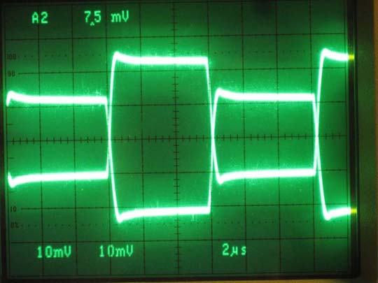
TIMING DELAY FOR MOSFETS
These are the gates drive signals going to the mosfets. The signals are superimposed. The small slope is part of the delay imparted by the series diodes D5 and D6.
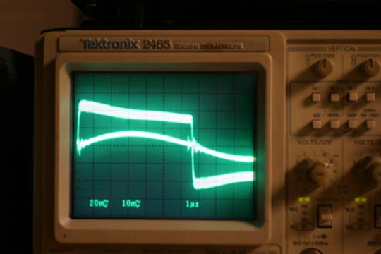
This is the inverter tracing on top, and one of the gate drive signals on the bottom. With this mosfet, when the gate is high the DS junction grounds the power, so the voltage drops to zero.

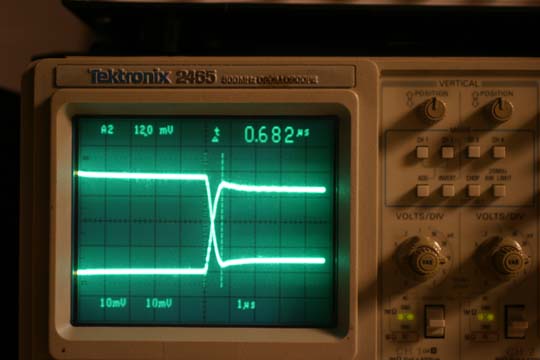
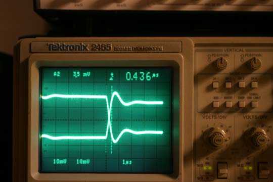
Below is the timing showing ZVS. The voltage goes through zero volts exactly when the current is zero.
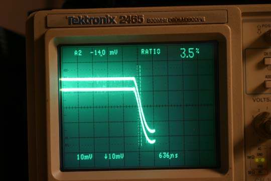
Below, one of the series diodes is shorted, so we can compare the timing of the signal going to both gates. The bottom tracing has the transformer gate drive going directly to the gate. The tracing above it goes through the diode The temporal difference between the gate drive with and without the series diode is close to 100ns.
Below are the gate drive waveforms with both series diodes working.
Below, both series diodes are shorted, and we can see the time to reach the same voltage is delayed by about 200ns.
OP-AMP INTEGRATOR
The op-amp is centered around Vdd/2. R10 moves the center point on the integrator allowing you to fine tune PLL frequency. You can force it to stay a little above resonance by adjusting it. When connecting it to the circuit, set it up so clockwise motion increases the PLL frequency.
MOSFETS, ZERO VOLT SWITCHING, and CURRENT MONITORING
Mosfets U1 and U2 have ultra-fast diodes across the source and drain to protect the slower acting intrinsic drain diodes. There are no series isolation diodes with the mosfets for two reasons. We are doing zero volt/current switching which is guarenteed when the circuit is in tune by the PLL. When we switch the mosfet there is no current or voltage on the device. Secondly, the present day mosfets have very fast intrinsic diodes, rated for flywheel service. Capacitors C1 and C2 set a point half-way above ground, which gets charged when U1 is open, and discharges to ground when U1 closes and U2 opens. The current transformer T2 uses a 1:100T ratio to monitor the inverter current. The 100R resistor means that every 1V on the oscilloscope is 1A of current going to the coupling transformer.
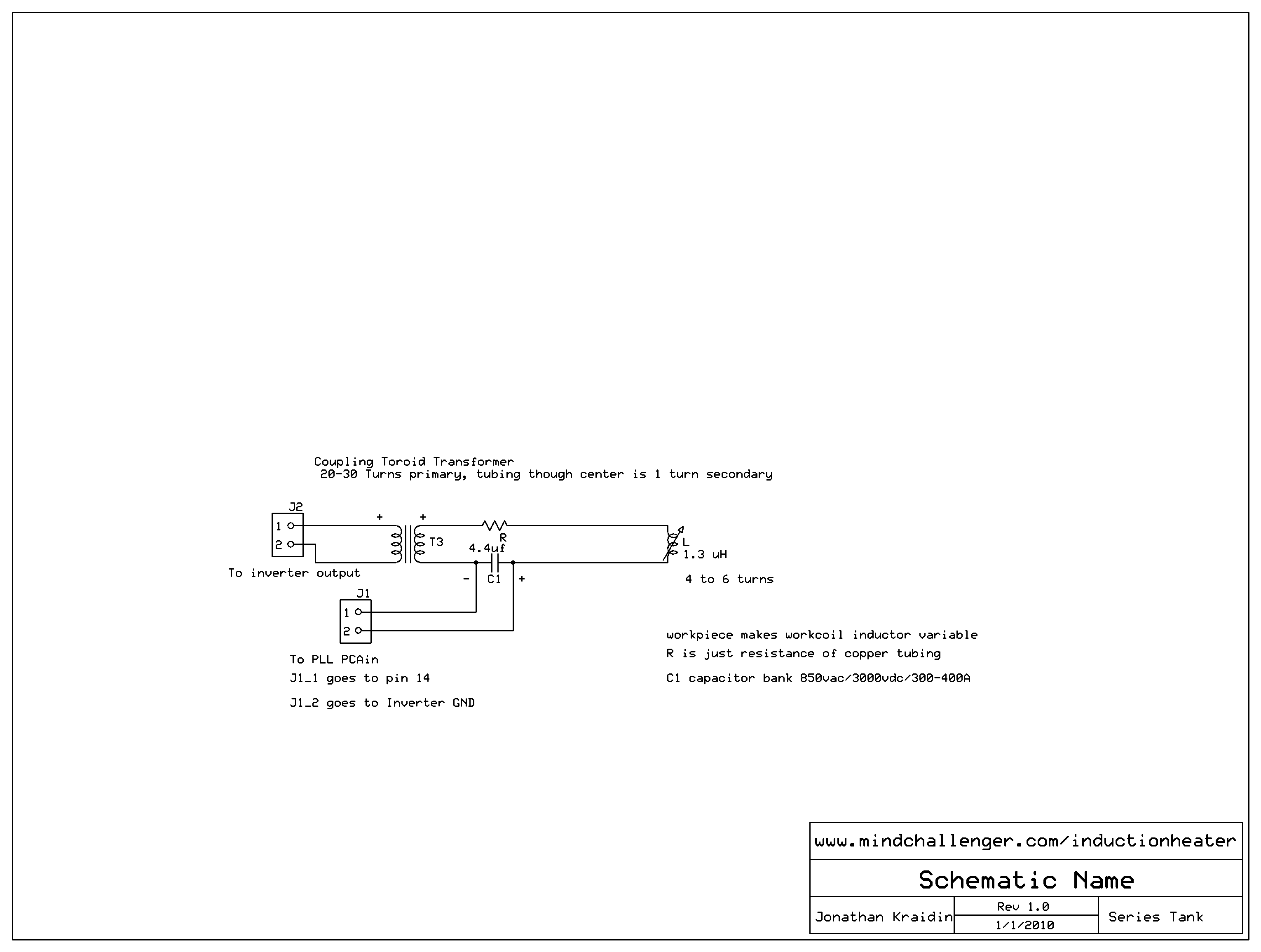
Now, let's look at the tank circuit schematic. The inverter output is coupled to the tank through T3, which is a 20:1 toroid transformer. The 20 turn primary is connected to the inverter output. The coper tubing which form the connects for workcoil and capacitor serves as a one-turn primary. You can experiment with different toroid materials and turn-ratios. The resonant frequency will changes as the material goes through its curie point.
Below is a picture of the current conduction through the inverter during different phases of the power transfer cycle. It shows how the free-wheeling diodes come into play to divert the reverse current around the mosfet.
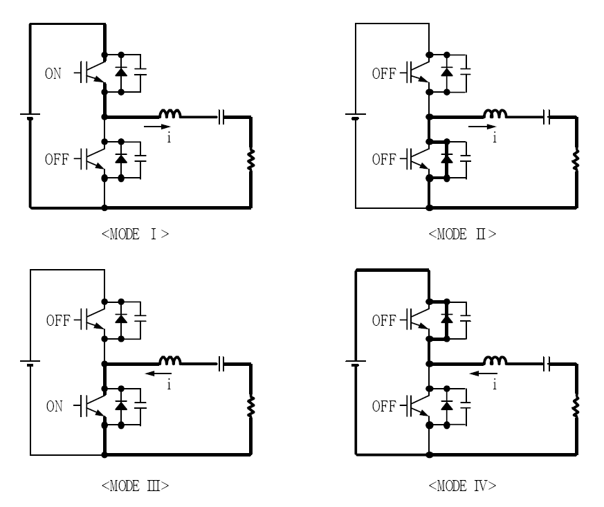
During Mode 1, the upper mosfet is conducting and transfering power to the resonant tank through the coupling transformer in our circuit. In Mode 2, the mosfets are transitioning, and the upper mosfet turns off slightly before the bottom one turns on. Here, current is conducted through the free-wheeling diode of the lower mosfet. In Mode 3, the lower mosfet turns on, and the resonant tank throws the power back through mosfet. In Mode 3, both mosfets are off during the transition, and the upper mosfet's free-wheeling diode conducts the current.
TUNING
You will have to tune the PLL to your tank's resonant frequency. To do this just connect jumper JP2. Leave jumper JP3 open, which goes to the integrator. With a volt meter, measure the voltage at pin 9 and the inverter ground. Trim R6 until you have one half of your supply voltage. Accounting for the diode voltage drop on the regulated 15vdc supply, this should be around 7.2v. You will need a differential set of oscilloscope probes to do this next part right. Put one probe pair across the current transformer, which would be across R15. Put another probe pair across the inverter output at J2. This will monitor inverter voltage and current. Using a variac, set the voltage input to your inverter high voltage supply to a low value like 30-40vac. Trim R5 until you have the current and voltage in phase. A cruder method uses an unregulated rectifier with a smoothing capacitor with the voltage input being the tank capacitor. Monitor the voltage for a maximum.
Once you are confident that the PLL's center frequency is close to the resonant frequency, open jumper JP2 and close jumper JP3. Turn on the inverter first and then turn on the variac to the voltage doubler, which provides the high voltage for the inverter. Slowly increase the voltage while monitoring the inverter voltage and current waveforms. After 20 or 30v you should see it lock onto Fres. The inverter output will be a nice square wave and the current will be close to a smooth sinusoidal tracing. If all you see is a triangle-looking wave for the current you probably have the polarity wrong on your capacitor voltage input to pin 14. The quickest fix is to swap the connections going to the coupling transformer. Try it again and it should work.
PLEASE NOTE THERE ARE MORE SCHEMATICS AT THE END OF THIS TUTORIAL (YOU HAVE MORE WEB PAGES TO GO)
You can watch a video of it working here.
If you have read this much, you might want to read a bit more. These two other sites are well worth the reading and explain things from their perspective with regards to the theory and construction of an induction heater.
Neon-John's Induction Heating Site
Tim Williams Index Link
Comments should go to jonathan_at_houseofficer.com
The next page shows images of the actual circuit.
PC Professor Computer Training, Service & SupportNOTE: There are more schematics for a higher powered unit at the end of this tutorial using microprocessor-controlled resonance locking.
This unit includes plans for levitating metals using high-powered magnetism.